1. Meet Monk9 Tech – India’s Legacy Chip Pioneer
Back in 2022, amid global chip shortages and tech sovereignty urgent calls, Monk9 Tech popped up in Rajkot, Gujarat. The mission? Democratize chip-making for Indian innovators—especially using older but still darn important nodes like 350 nm and 180 nm.
2. Why Legacy Nodes Still Matter
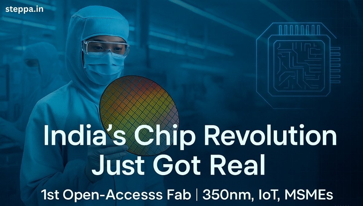
Cutting-edge chips (5 nm, 7 nm) are cool, but not every gadget needs them. Legacy nodes power a ton of real-world stuff—think IoT sensors, automotive electronics, defence gear, and factory automation . Monk9’s fab focuses on 6-inch wafers at 350 nm—the first open-access fab of its kind in India.
3. Team Behind the Vision
Founder Marmik Bhatt, who knows chip design and automation inside out, named the company “Monk9” to reflect deep thinking (“Monk”) and innovation (“9”). His dream: affordable fab access for startups, MSMEs, tier-2 colleges, and labs.
4. How Monk9 Supports Builders
They’ve got tier-based pricing—cheap for academia, market-aligned for industry. Their users? Early-stage startups, small colleges, MSMEs—all who’ve struggled with overseas fab costs and delays.
5. Open-Source to the Core
They’re using tools like Efabless OpenLane, Sky130 PDKs, and open RTL-to-GDS flows. This open-hardware model speeds up prototyping and lowers barrier for designers:
“Open-source gave us the springboard we needed… iterate quickly and educate users.”
6. Big Market & Money Moves
India’s legacy chip demand (IoT + automation) sits north of ₹15,000 crore. Monk9 plans to serve it with fab access, tape-out bundles, prototyping, IP licensing, and design training. Alliances with universities, and government and industry schemes—are part of the game plan n.
7. Ecosystem Support & Early Wins
They’re backed by big names: FITT-IIT Delhi, IIMA Ventures, RK University, and Gujarat’s electronics policy. They also work with global networks like Efabless (Palo Alto). On their to-achieve list:
- MoUs with universities
- Validated UART, ALU, VGA IP cores
- Cleanroom layout, pilot fab plans ready
- Near-term: production ready 350 nm line, 20 first design customers, roll out of PDK V1.0
8. Challenges They’ve Faced
- Finding refurbished fab equipment
- Forming a team that can run a semiconductor fab
- Navigating technical hurdles
But Bhatt says:
“Start lean, iterate fast, keep your mission rooted in real needs.”
9. What’s Next? Full-Stack Ambitions
Beyond 350 nm, Monk9 dreams of moving into 180 nm and 130 nm, plus packaging, testing, and scaling up—ultimately building India into a full-fledged fabrication hub .
10. Myth vs. Truth: Setting Things Straight
| Myth | Truth |
| “India doesn’t need legacy fabs.” | False—legacy nodes are critical for mass-market IoT and auto. |
| “Fab access is only for big players.” | Monk9 makes it affordable for small outfits and colleges. |
| “Open-source isn’t reliable.” | It’s proven and flexible—Monk9 speeds development with it. |
Final Take
Monk9 Tech isn’t chasing bleeding-edge glory. They’re tackling a massive, practical gap: affordable chip manufacture for real-world needs. They’re bringing fab infrastructure to innovators, not just big names. If they pull off full operations later this year, India takes a giant leap toward chip independence. Honestly? It’s bold—and exactly what we need.
To wrap it up—Monk9 Tech is starting small but thinking big. India’s semiconductor journey starts here.
Also read: India Invites Cisco to Power Up AI, 6G & Digital Growth — What It Really Means